My first ZMK Planck, Part 2 — The alignment
Part 1 ended on an idea: the keyboard holds nothing but the matrix, and the controller and battery live on a detachable bar along the rear edge.
That sentence hides all the work. A passive matrix only becomes a keyboard when sixteen signals reach a controller — so the bar is not a mounting bracket, it is a connector problem wearing a bar costume.
Sixteen, and a joint that comes apart
4 rows + 12 columns = 16 signals, and the controller has exactly 16 usable GPIO. No spare, no ground return, no detect pin.
And the joint has to come apart — that is the whole point of the bar. So those sixteen make and break contact by hand, repeatedly, and have to be right every time.
Matrix lines are unforgiving in one specific way. They are high-impedance with internal pull-ups, so contact resistance costs nothing. What kills you is an intermittent open: one pin that loses contact under flex gives you a column that dies when you press on the case and comes back when you let go. On a handwire that looks exactly like a bad solder joint, and you will go hunting through 48 of your own joints before you suspect the connector.
Why that way, and why not the others
Bonded — sixteen wires, no connector. Most reliable thing available. Rejected: it throws away the reason the bar exists. If the controller dies, you desolder sixteen wires.
One 2x8 header in the centre. On paper the best option — keyed, retained, self-aligning, one alignment datum instead of two. Rejected on looks. The factory opening sits at the right rear; a centre connector means cutting a fresh hole mid-edge while the original does nothing. On frosted translucent acrylic there is no back side to hide that on.
Two 1x8 headers at the ends. Shorter runs, still keyed and retained, but two connectors to mate and you have to push them together.
Two 1x8 magnetic pogo connectors at the ends. Quick-release, no insertion force. Also the riskiest thing on the list, and I was told so in plain terms:
- Tolerance stack-up. Two connectors ~250 mm apart seating at once, on a hand-built bar, against acrylic that bows. Magnets self-align over maybe ±0.3 mm — easy to end up with one home and the other marginal.
- No wipe, no retention. Pogo tips oxidise, and a magnet joint has no wiping action and nothing holding it but the magnet.
- Magnets next to a radio. Neodymium along the rear edge detunes the chip antenna. Keep 10–15 mm clear or lose range.
All three are correct. None of them is a cost I mind paying.
The alignment problem is the exercise — I am already betting the build on placing things accurately by hand, so a connector that punishes sloppiness just puts a pass/fail light on it. The wear is real, but every smartwatch I own charges through pogo pins and lives on a wrist, outdoors, in sweat; this one sits on a desk mat under a roof, and when the contacts eventually go they are a consumable. And the range: the link is half a metre to the PC, less to a dongle in the same machine, against a spec written for tens of metres. Lose half of it and I am still an order of magnitude clear.
So I bought the pogo. The trade-offs land somewhere I do not care about.
The one thing I would not trade is what crosses the joint: signals only. No battery, no VCC, no ground rail. The cell lives on the bar beside the controller it powers, and nothing on the keyboard side is energised at all. Push power through a magnetic connector and every reseat is a chance to short a cell across a pin that landed half-on, or brown out the controller mid-write. A bad contact on a matrix line is a missing keypress. That is the whole difference between “annoying” and “damage,” and it is the one line in this design I would keep in any version of it.
Two holes, and then the case is finished
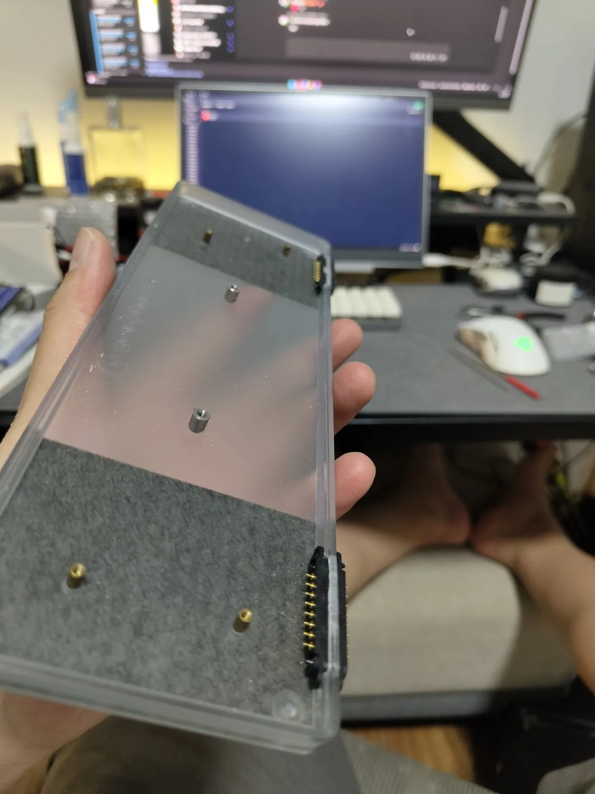
Two cuts in the end. The factory opening at the right rear got extended to take the first connector alongside the port it was always for. The second is new, cut at the opposite end to match.
That is why the centre header lost and this did not. The objection was never “no new holes” — it was leaving the original hole orphaned while cutting a redundant one somewhere else. Extend one, mirror it at the far end, and the rear edge reads as a pair rather than as one useful opening and one mistake.
The corner placement was deliberate too, and it is the part of the design I had the clearest picture of before building any of it. Both connectors sit hard against the corners, where the side walls meet the plate and the acrylic is stiffest. A snap-on bar lives or dies on the panel it snaps to holding still, and the centre of a 250 mm span is the one place guaranteed not to. Two datums are worse than one in principle — but mine sit where the case barely moves, and the single-datum version would sit where it moves most.
There is no drawing of any of this. The whole mechanism lived in my head, the way these things always do for me, and the first time it existed outside my skull was when I started cutting. Lovely right up until something does not fit and there is no document to check your intent against. That bill comes due in Part 5.
With the plate cut and both connectors mounted, the case is done. Nothing else will ever be modified. Everything after this is wire.
The matrix
Sixteen signals, two connectors, eight each — each connector landing on the controller pad rail nearest it.
The obvious 8/8 split is wrong, though, because of what the right rail offers. Two of those pads are the nRF52840’s NFC antenna pins. They work as GPIO, but only with a build-time flag that takes them off the NFC peripheral, and they carry a reputation for odd behaviour. On a board where a flaky column was already going to be hard to localise, I was not spending credibility on two pins with an asterisk.
So: 10 pins on the left rail, 6 on the right, NFC pads untouched. The price is two wires crossing the width of the bar to reach the far rail. Two crossings is cheap; debugging an NFC pin is not.
| Connector | Carries | Lands on |
|---|---|---|
| A (left end) | R1, C1, C2, R2, C3, C4, C5, C6 | D1, D0, D2, D3, D4, D5, D6, D7 — left rail |
| B (right end) | C7, C8, C9, C10, R3, R4 | right rail |
| B (left end) | C11, C12 | D9, D8 — crossing to the left rail |
Diode direction
A diode at every switch, and all 48 pointing the same way. Which way is a free choice, as long as you tell the firmware the same story you told the soldering iron — ZMK calls it diode-direction and takes col2row or row2col (kscan configuration).
I wired col2row.
Note for the firmware phase:
diode-direction = "col2row". This is a one-line property in the shield’s devicetree, and getting it backwards produces a board that scans cleanly and reports the wrong keys — or nothing. Write it down now. Part 3 needs it, and the matrix is about to become unreachable under a plate.
Two kinds of wire, for two different reasons
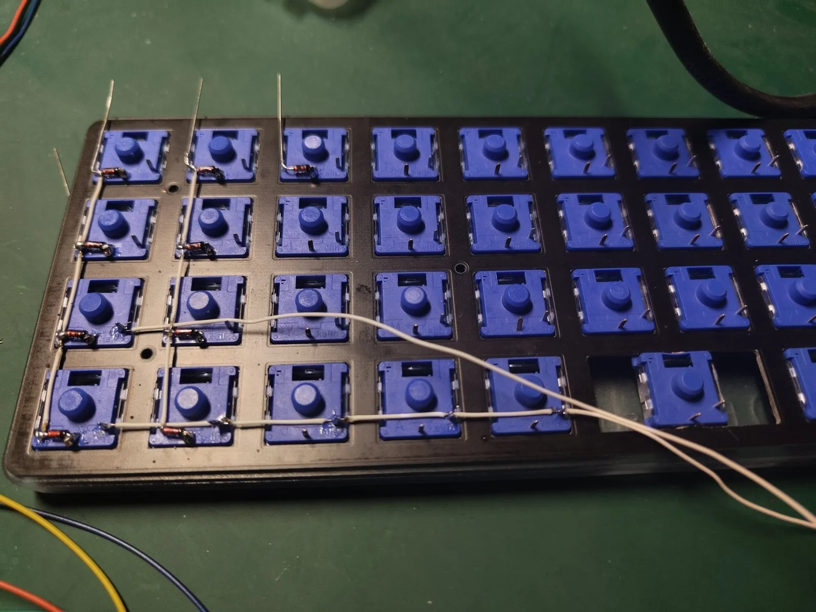
The white wire is the matrix grid, and it is routed for looks. The case is frosted acrylic over a black plate, which means the underside of this keyboard is visible — not in an exploded-photo sense, in an it-is-on-my-desk sense. So the crossings are deliberate: evenly spaced, square to the plate, white against black so the grid reads cleanly from below. It is a keyboard you can see the inside of, so the inside gets laid out like something meant to be seen.
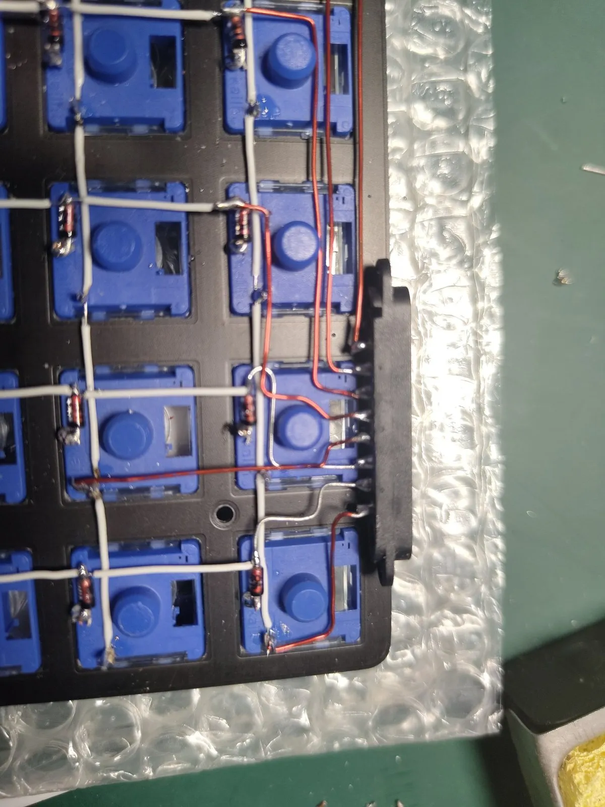
The red is doing a completely different job. It is single-core brass in a ceramic wrap: bends easily by hand, then stays exactly where you bent it. Those are the sixteen runs that leave the matrix, and because the wire holds its shape it does more than carry signal — it is stiff enough to hold the pogo connector in position at the edge.
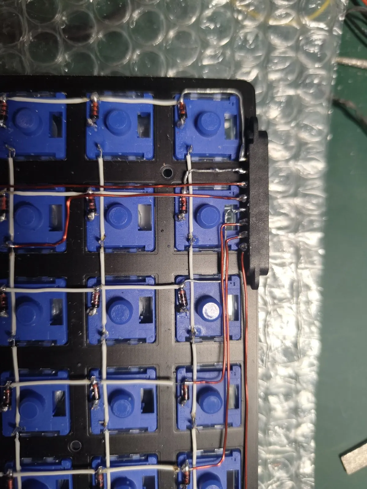
That matters more than it sounds. Pulling the bar off means pulling against magnets, and the connector on the keyboard side has to not move when you do. Its own wiring braces it. Sixteen stiff wires converging on a block, routed to resist the one direction the magnets pull.
Sealed
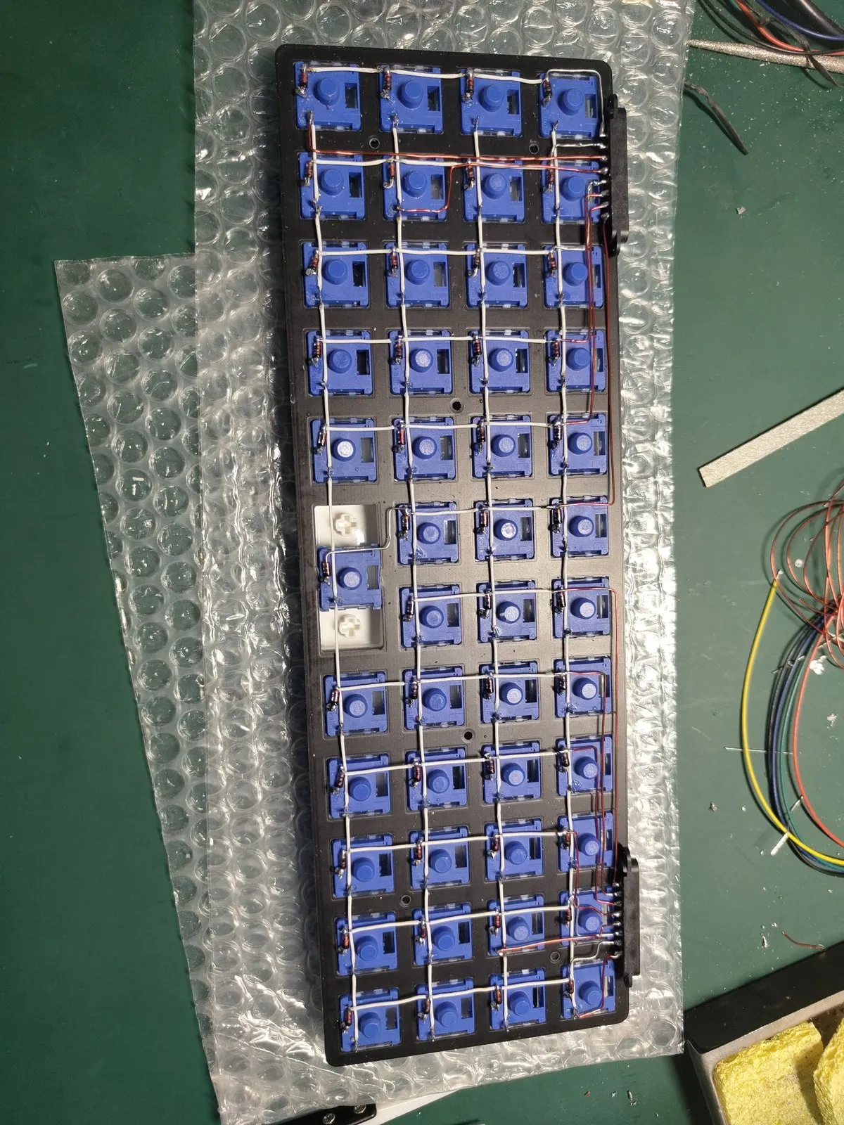
That is the end of Part 2, and it is a strange place to stop, because look at what is not in that photo.
There is no controller. Not an empty socket waiting for one — nothing. The case is cut, the connectors are mounted, all 48 keys are wired and verified, and the board is complete in the only sense that matters: nothing else needs to happen inside it, ever.
And I still had not chosen a controller.
That was not procrastination. The matrix is not committed to a board, it is committed to a pinout convention — the pro micro pad layout, which half the hobby builds against and which ZMK addresses through aliases rather than hardware names. Any board that speaks that layout will do. I did not decide what the controller is. I decided that it would not matter.
Which is a nice thing to say in a blog post and a better thing to have actually done, because in Part 4 I throw two controllers in the bin and the matrix never notices.
Part 3 — the planck_choc shield, a repo holding two keyboards at once, and building Zephyr in a container on Windows.